Articles > Precious Metal Properties (PMP)
Indium phosphide (InP) plays a crucial role in optical communications due to its numerous applications and importance. One of the significant uses of InP is as a light source in optical communication systems. InP-based laser diodes provide high-performance light emission, making them suitable for transmitting information over long distances. These laser diodes are essential components in fiber optic communication devices, where they facilitate the efficient transfer of data through optical fibers.
Moreover, InP offers a lossless transmission method for connecting computers in optical communication networks. Its low optical attenuation properties ensure minimal signal loss, resulting in reliable and high-quality data transmission. This makes InP an ideal choice for establishing stable connections between computing devices.
Furthermore, InP exhibits a wide range of wavelengths that can be utilized in fiber optic communication devices. This versatility allows for the efficient transmission of data over different wavelengths, maximizing the capacity and speed of communication systems. InP-based devices can operate at various wavelengths, providing flexibility in routing and managing optical signals.
Lastly, InP holds immense potential for future electronics due to its unique properties. Its remarkable electron mobility and high electron velocity make it suitable for high-frequency and high-speed electronic devices. InP-based transistors and integrated circuits are predicted to revolutionize the field of electronics, enabling the development of faster and more efficient computing systems.
In conclusion, indium phosphide (InP) is a critical material in optical communications. Its applications as a light source, lossless transmission method, and its wide range of wavelengths make it indispensable in fiber optic communication devices. Additionally, its potential for future electronics highlights the importance and significance of InP in advancing communication and computing technologies.
Introduction: The History of InP in Communication Technologies
Indium Phosphide (InP) has played a significant role in the field of communication technologies over the years. With its unique electrical and optical properties, InP has revolutionized the way information is transmitted, enabling faster, more efficient, and reliable communication systems. This article will explore the history of InP in communication technologies, from its discovery and early applications to its current and future contributions. We will delve into the key advancements that have made InP a preferred material for various communication components, such as lasers, photodiodes, transistors, and integrated circuits. Additionally, we will discuss the notable milestones and breakthroughs that have propelled the adoption of InP in telecommunications, wireless networks, fiber-optic communications, satellite communications, and other areas. By understanding the evolution of InP in communication technologies, we can appreciate its immense impact on our connectivity-driven world and anticipate the exciting developments that lie ahead.
The evolution of InP (Indium Phosphide) technology in the field of optical communications has been remarkable, with its increasing application in both telecom and data centers. InP technology has played a crucial role in enhancing data transmission capabilities and enabling the reliable and efficient flow of information.
One of the major advantages of InP Photonic Integrated Circuits (PICs) is their ability to increase data rates. InP PICs allow for the integration of various components, such as lasers, modulators, and detectors, onto a single chip. This integration enables higher data transmission speeds, as the signals can be processed and transmitted more quickly and accurately.
Another advantage of InP PICs is their ability to enable multiplexing, which allows multiple signals to be transmitted simultaneously over a single optical fiber. InP technology provides the capability to integrate multiple wavelength channels, enabling higher bandwidth and increased data capacity. This is particularly important in data centers and telecom networks where the demand for data transmission continues to grow rapidly.
Energy efficiency is also a key advantage of InP PICs. The integration of various components onto a single chip reduces power consumption and enables more efficient use of resources. This is particularly important in data centers, where power consumption can be a significant portion of operational costs.
Several key players in the industry have contributed to the development of InP-based optical transceivers. Companies such as EFFECT Photonics have been at the forefront of this technology, developing innovative InP PICs that have revolutionized optical communications. Their contributions have not only improved data transmission capabilities but also enabled more cost-effective and energy-efficient solutions.
In conclusion, the evolution of InP technology in the field of optical communications has been instrumental in enhancing data rates, enabling multiplexing, and improving energy efficiency. This technology has been a game-changer in the telecom and data center industry, and companies like EFFECT Photonics continue to drive innovation and advance the capabilities of InP-based optical transceivers.
InP (indium phosphide) offers distinct advantages over other materials when it comes to communication devices. Firstly, it is known for its ability to produce highly efficient lasers, making it a preferred choice for telecommunications applications. The lasers made from InP exhibit high power output and low energy consumption, ensuring optimal performance and cost-effectiveness.
Secondly, InP is highly suitable for producing sensitive photodetectors. These photodetectors are crucial in communication devices as they convert light signals into electrical signals, enabling efficient data transmission. InP photodetectors provide excellent sensitivity, ensuring accurate and reliable data detection.
Lastly, InP is used for producing modulators, which are essential components in communication devices for encoding and decoding signals. InP modulators offer high-speed performance, allowing for fast data processing and transmission. This makes them ideal for applications in telecommunications, where high data rates are required.
It is worth noting that InP lasers find applications in various communication networks, including metro ring access networks, free space satellite communication, and connections to wireless 3G, LTE, and 5G base stations. Their efficiency and reliability make them crucial for enabling high-speed and high-capacity data transfer in these networks.
In conclusion, the advantages of using InP for communication devices include the ability to produce efficient lasers, sensitive photodetectors, and high-speed modulators. These advantages make InP an ideal material for telecommunications applications, ensuring optimized performance, accurate data detection, and reliable signal modulation.
Introduction:
Indium Phosphide, commonly known as InP, is a semiconductor material that possesses unique properties making it ideal for a wide range of applications in the field of electronics and optoelectronics. InP exhibits remarkable electronic and optical characteristics that make it highly suitable for devices such as transistors, lasers, photodetectors, and solar cells. Its superior properties, including a direct bandgap, high electron mobility, high thermal stability, and excellent radiation resistance, contribute towards its widespread use in various technological advancements. In this article, we will delve into the properties of InP material, exploring its structure, electrical behavior, optical properties, and other key aspects that make it an invaluable material in the world of semiconductors.
Source:
- Vurgaftman, I., Meyer, J. R., & Ram-Mohan, L. R. (2001). Band parameters for III–V compound semiconductors and their alloys. Journal of applied physics, 89(11), 5815-5875.
InP modulator technology boasts high electron mobility and low noise characteristics, making it a crucial technology for next-generation high port density coherent systems. The high electron mobility of InP materials enables fast and efficient movement of electrons, allowing for high-speed signal processing and data transmission.
This high electron mobility plays a vital role in coherent systems, where multiple channels of information need to be transmitted simultaneously. The ability to process large volumes of data quickly and accurately is essential for meeting the demands of modern communications systems.
Moreover, low noise levels are crucial for preserving the integrity of transmitted signals in high-port density systems. Noise can degrade the quality of the signal and affect its ability to carry information efficiently. The low noise characteristics of InP modulator technology ensure that the transmitted signals remain clear and intact, ultimately enhancing the overall performance of the system.
These impressive characteristics are enabled by the InP platform and advanced material engineering capabilities. InP, or indium phosphide, provides an excellent platform for building high-performance optoelectronic devices due to its favorable electronic properties. The material engineering capabilities associated with InP platforms enable precise control over material properties, such as doping and interface characteristics, enhancing their performance.
In conclusion, the high electron mobility and low noise characteristics of InP modulator technology are crucial for next-generation high-port density coherent systems. Enabled by the InP platform and advanced material engineering, these characteristics ensure efficient signal processing and transmission, ultimately enhancing the performance of modern communication systems.
Wide bandgap materials, such as silicon carbide (SiC) and gallium nitride (GaN), possess a wider energy bandgap compared to traditional silicon. The bandgap refers to the energy difference between the valence and conduction bands in a material. Wide bandgap materials have bandgaps greater than 1.0 electron volt (eV), while silicon has a bandgap of 1.1 eV. This wider bandgap allows for higher breakdown voltages, better thermal stability, and improved power handling capabilities.
In terms of thermal conductivity, wide bandgap materials also exhibit exceptional properties. Silicon carbide, for example, has a thermal conductivity of around 350 W/mK, which is significantly higher than silicon's thermal conductivity of approximately 150 W/mK. High thermal conductivity enables efficient heat dissipation, ensuring that electronic devices can operate at higher power levels without overheating.
Wide bandgap materials offer significant advantages over traditional silicon in terms of power capabilities and efficiency. Their wider bandgap allows these materials to withstand higher voltages, making them suitable for high-power applications. Additionally, wide bandgap materials have lower switching losses, enabling converters and inverters to operate at higher frequencies and achieve higher efficiencies.
Examples of wide bandgap materials used in various electronic applications include silicon carbide (SiC) and gallium nitride (GaN). SiC is commonly used in power electronic devices such as high-voltage rectifiers, inverters, and power modules. Its high thermal conductivity ensures efficient heat dissipation, reducing the risk of thermal damage. GaN, on the other hand, is often utilized in high-frequency and high-power devices such as radio frequency amplifiers and power converters. GaN's high thermal conductivity facilitates effective cooling, maintaining stable operation under demanding conditions.
In conclusion, wide bandgap materials like silicon carbide and gallium nitride offer significant advantages over traditional silicon in terms of power capabilities and efficiency. Their wide bandgap allows for higher breakdown voltages, better thermal stability, and improved power handling. Moreover, their high thermal conductivity enables efficient heat dissipation, ensuring reliable operation at higher power levels. These exceptional properties make wide bandgap materials crucial components in various electronic applications.
Introduction:
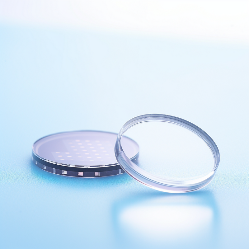
InP, short for Indium Phosphide, is a compound semiconductor material that has gained significant prominence in the field of optical communications. This material exhibits excellent optical and electronic properties, making it highly suitable for various applications within the telecommunications industry. In this article, we will explore the wide range of applications of InP in optical communications, including its use in fiber optics, laser diodes, photodetectors, and integrated circuits. By harnessing the unique properties of InP, researchers and engineers have been able to revolutionize the way information is transmitted and processed, leading to faster, more reliable, and more efficient communication systems. Let us delve deeper into the specific applications and understand the impact that InP has had on the field of optical communications.
Silicon photonics technology has emerged as a promising solution for high-speed data transmission in laser diodes. Laser diodes are widely used in various applications, including telecommunications, optical interconnects, and data centers, as they can generate coherent and intense beams of light.
The integration of silicon photonics with laser diodes allows for improved performance and efficiency. The use of silicon as a platform for laser diodes enables the miniaturization of devices and enhances their speed and bandwidth capabilities. Silicon photonics provides a highly compatible and scalable solution for high-speed data transmission due to its ability to integrate with existing silicon-based electronic devices.
One key advantage of silicon photonics in laser diodes is its power efficiency. Silicon-based optical devices can operate at lower power levels while maintaining high-speed data transmission, reducing the energy consumption significantly. This is crucial for data centers and other applications where power consumption is a critical factor.
Silicon photonics also offers enhanced temperature stability. Silicon-based materials have excellent thermal properties, making them less susceptible to temperature-induced fluctuations that can degrade laser diode performance. This stability improves the reliability and longevity of laser diodes, ensuring consistent high-speed data transmission even in challenging operating conditions.
Additionally, the integration capability of silicon photonics enables the production of highly integrated systems. Combining both electronic and photonic functionalities on a silicon chip allows for compact and cost-effective solutions. It streamlines manufacturing processes and facilitates the development of complex optical systems, promoting widespread adoption of high-speed data transmission technologies.
To summarize, the use of silicon photonics in laser diodes for high-speed data transmission offers several advantages, including improved performance and efficiency, reduced power consumption, enhanced temperature stability, and increased integration capabilities. This technology holds great potential for revolutionizing the field of optical communications and addressing the ever-growing demand for faster and more reliable data transmission.
Integration with silicon photonics plays a crucial role in enhancing the performance of coherent transmission systems. By leveraging the inherent properties of silicon, such as its high refractive index and low material loss, integration with silicon photonics enables the development of compact and efficient devices.
One of the key benefits of using silicon photonics is the reduction in development time. Silicon is a well-established material in the semiconductor industry, and its compatibility with existing fabrication processes allows for faster prototyping and production cycles. This leads to shorter time-to-market for coherent transmission systems.
Additionally, silicon photonics enables higher levels of integration. Through the use of advanced fabrication techniques, multiple optical components such as modulators, detectors, and multiplexers can be integrated onto a single silicon chip. This integration not only reduces device size but also simplifies the assembly process, resulting in fewer manual assembly steps.
Silicon-based photonic integrated circuits (PICs) further enable the density required for pluggable coherent modules. By integrating all the necessary components onto a single chip, PICs reduce the space required for assembly. This directly translates into a reduction in both cost and size compared to discrete components.
Moreover, PICs eliminate the need for external polarization control components. The high refractive index of silicon ensures strong optical confinement, making it highly insensitive to polarization. This eliminates the need for manual polarization alignment and external components, further simplifying the system and reducing cost.
In conclusion, the integration with silicon photonics in coherent transmission systems brings numerous benefits, including reduced development time, higher levels of integration, and fewer manual assembly steps. Additionally, silicon-based photonic integrated circuits enable the density required for pluggable coherent modules, reduce cost and size, and eliminate the need for external polarization control components.
Introduction:
III-V materials, such as indium phosphide (InP), are increasingly gaining significance in various technological applications. These materials are composed of elements from group III (such as indium) and group V (such as phosphorous) in the periodic table, possessing unique properties that make them highly desirable for use in various electronic, optoelectronic, and photonic devices. The importance of III-V materials like InP lies in their exceptional attributes, which include high electron mobility, direct bandgap, and superior thermal conductivity. These properties enable III-V materials to serve as the foundation for the development of high-performance devices such as transistors, lasers, solar cells, and photodetectors. Additionally, III-V materials also offer advantages such as excellent light absorption, fast carrier dynamics, and compatibility with silicon-based technologies. Thus, the exploration and utilization of III-V materials like InP hold immense importance in advancing the fields of electronics, photonics, and renewable energy technologies.
When it comes to traditional materials, two prominent ones that come to mind are silicon and gallium arsenide. Both materials have been extensively used in various industries, but they have significant differences in terms of their properties and applications.
Silicon is perhaps the most well-known and widely used traditional material. It is a semiconductor that has excellent thermal stability and is abundant in nature. Silicon is commonly used in electronic components such as transistors and integrated circuits. Its abundance, cost-effectiveness, and adaptability make it a preferred choice for many industries. Silicon also has a wide bandgap, making it suitable for high power applications.
On the other hand, gallium arsenide (GaAs) is a compound semiconductor that offers superior electrical properties compared to silicon. GaAs has a higher electron mobility, which means it can operate at higher frequencies and with lower noise levels. This property makes it ideal for high-speed applications such as satellite communication, radar systems, and photovoltaic devices. GaAs is also more resistant to radiation than silicon, making it suitable for use in space applications.
In summary, the key differences between silicon and gallium arsenide lie in their electrical properties, cost-effectiveness, and applications. Silicon is widely used in industries due to its abundance and adaptability, particularly in electronic components. On the other hand, gallium arsenide excels in high-speed applications and has enhanced resistance to radiation, making it suitable for aerospace and satellite communication systems.
III-V materials, a class of compound semiconductors composed of elements from groups III and V of the periodic table, play a crucial role in advancing communication technologies. They have unique properties that make them highly desirable for a range of applications, including optoelectronics and high-speed wireless communication.
One significant contribution of III-V materials in communication technologies is their ability to grow epitaxial layers on silicon substrates. Silicon is the dominant material used in integrated circuits, but its optical and electronic properties are limited. By depositing III-V materials, such as gallium arsenide (GaAs) or indium phosphide (InP), on silicon substrates, it is possible to combine the best attributes of both materials. This process, known as heteroepitaxy, allows for the integration of high-speed transistors and lasers with the existing silicon technology.
Among the III-V materials, gallium phosphide (GaP) holds particular promise as a successful semiconductor. GaP has a direct bandgap, making it suitable for efficient light emission and absorption. This property makes GaP highly attractive for the development of high-performance optoelectronic devices such as lasers and light-emitting diodes (LEDs). Additionally, GaP exhibits excellent thermal stability, enabling it to withstand high-temperature processing, offering opportunities for advanced device fabrication.
In summary, III-V materials are instrumental in advancing communication technologies due to their ability to grow epitaxial layers on silicon substrates and the potential of particular semiconductors like GaP. These materials enable the integration of high-speed transistors and lasers with existing silicon technology, leading to improved performance and new possibilities for optoelectronics.
Introduction:
Eindhoven University of Technology (TU/e) is globally renowned for its excellence in research and development (R&D) activities. With a strong focus on engineering and technology, TU/e has established itself as a leading institution that fosters cutting-edge innovation and drives advancements across various fields. This institution’s commitment to R&D is evident through its state-of-the-art laboratories, extensive research partnerships, and diverse interdisciplinary collaborations. The university's dedication to pushing the boundaries of knowledge and translating research findings into tangible solutions is reflected in its dynamic research ecosystem. Underpinning TU/e’s R&D efforts are a talented team of researchers, faculty members, and students who work tirelessly to tackle real-world challenges and spearhead breakthrough discoveries. Below, we delve into some of the key areas of research and development at Eindhoven University of Technology.
InP (Indium Phosphide) technology has made significant contributions to the advancement of the telecom sector, particularly in the field of optoelectronics. InP lasers, in particular, have been increasingly applied in various applications such as metro ring access networks, satellite communication, and wireless base stations.
One of the key contributions of InP technology is its ability to enable high-speed and high-performance optical communication systems. InP lasers, with their wide bandwidth and low loss properties, have revolutionized the telecom sector by providing faster and more reliable data transmission. They have enabled the deployment of high-capacity fiber optic networks that can handle massive amounts of data and support bandwidth-intensive applications.
Furthermore, InP lasers have been instrumental in the development of metro ring access networks, which are essential for connecting multiple local networks over a wide area. They have also been employed in satellite communication systems, enabling high-speed and low-latency communication between satellites and ground stations. In addition, they have found applications in wireless base stations, where they provide efficient wireless communication over long distances.
One of the key advantages of InP chips is their ability to increase data rates through multiplexing. This means that multiple streams of data can be combined and transmitted simultaneously, allowing for faster data transmission. Additionally, InP chips are extremely energy efficient compared to electronic systems. This enables significant cost savings and reduces the carbon footprint of telecom networks.
In conclusion, InP technology, particularly InP lasers, has played a crucial role in the advancement of the telecom sector. Its contributions include enabling high-speed optical communication systems, supporting various applications, and providing advantages such as increased data rates and energy efficiency. As the demand for faster and more reliable communication continues to grow, the importance of InP technology will only continue to increase.
 Author: Guava AU